- 端末にloginする。
Loginしたら、ターミナルを開く(画面下部のツールバーの端末のアイコンをクリック) - ローカルで実行する場合
- .cdsinit を編集
editor="/usr/local/bin/mule" から editor="vi"へ変更 - レイアウトツールの起動
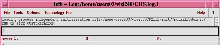
hp01% icfb &
- .cdsinit を編集
- リモートで実行する場合
- 端末の環境の設定
% xhost +usr1 +usr2 - usr1.vdec.u-tokyo.ac.jp もしくは usr2.vdec.u-tokyo.ac.jp に remote login する。アカウント名パスワードは端末と同じ
% rlogin usr1.vdec.u-tokyo.ac.jp -l vlsi2** (**は各自のユーザIDによって異なる)
Password: ********
usr1% - 環境変数の設定
usr1% setenv DISPLAY hp**.vdec.u-tokyo.ac.jp:0 (**は各端末の番号:モニターのラベルを参照すること) - レイアウトツールの起動
usr1% icfb &
- 端末の環境の設定
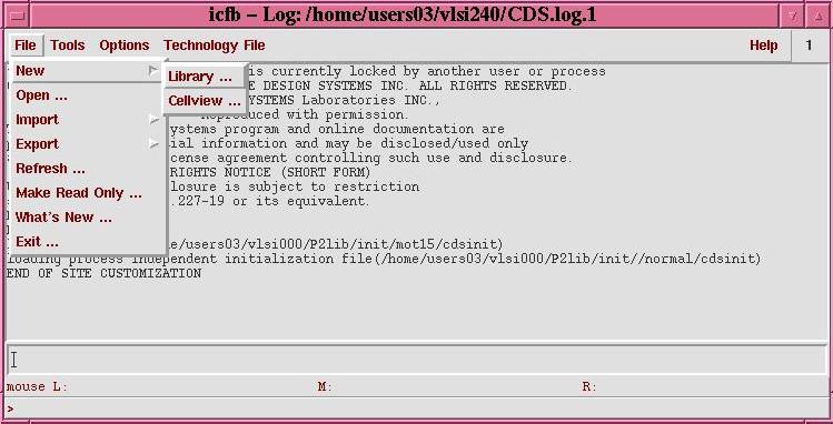
- File > New > Library の実行
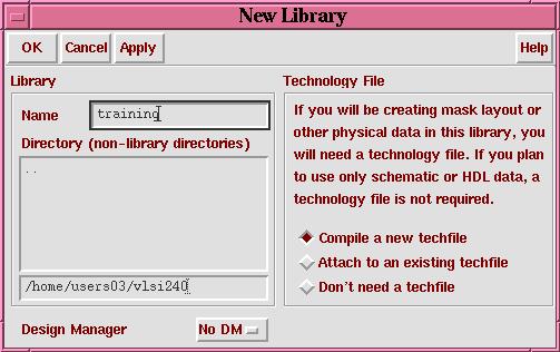
- Library Name を適当に決める(ここでは training)
- Compile a new techfileが選択されていることを確認してOKをクリック
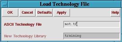
- ASCII Technology File に mot.tf を指定し、OKをクリック
- File > New > Cellview
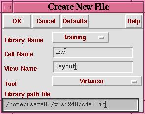
- Library Name: training(先程作成したライブラリ名), Cell Name: inv (ここではインバータを作成する), View Name: layout, Tool: Virtuosoと指定し、OKをクリック
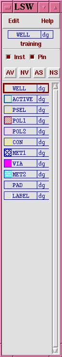
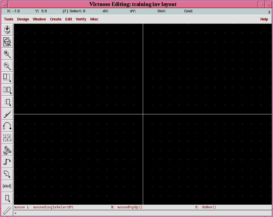
- エディタウインドおよびLSWウィンドウが起動
- プロパティの変更(Design > Options > Display)
Display Levels: From:0, To: 2 Grid Cotrols X Snap Spacing: 1 Y Snap Spacing: 1 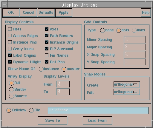
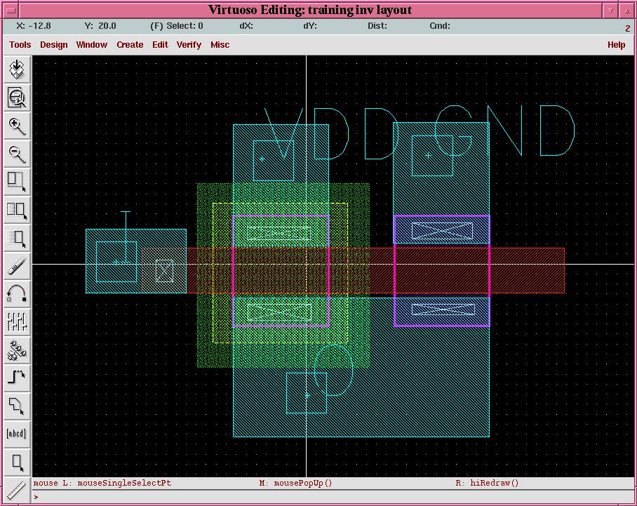
- Rectangle(Create > Rectangle: r), Polygon(Create > Polygon: p)などを用いて図形を編集
- Undo(Edit > Undo: u), Move(Edit > Move: m), Copy(Edit > Copy: c), Stretch(Edit > Stretch: s)コマンド等を用いて適宜図形の編集を行なう
- Create > Pin:を用いて端子を作成する。
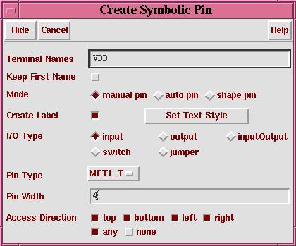
Terminal Names: 適当な端子名(ただし電源は vdd!, グランドは gnd!)
Create Labelを選択
Pin Tyle: ピンを付加する配線に合わせて MET1_T, MET2_Tを選択
- Set Text Style をクリック
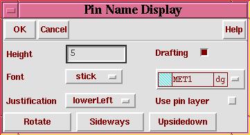
レイヤーを配線レイヤーに合わせる
Heightは適当な大きさになるように調整する
- 設計規則検査(Verify > DRC)
検査用ファイルのコピー:usr1% cp ~vlsi240/training/divaDRC.rul ~/training 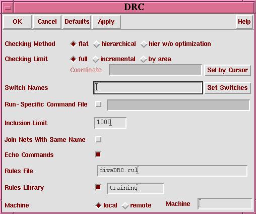
Checking Method: flag Checking Limit: full Rules File: divaDRC.rul Rules Library: training これでOKを押すと、エラーの箇所にマークが出るとともに、LOGが以下のようになるので、これが なくなるようにレイアウトの修正を行なう。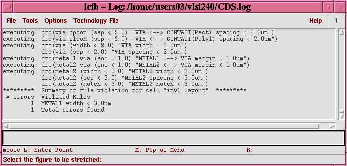
- Design > Save
- Window > Close
- 抽出ルールファイルのコピー
usr1% cp ~vlsi240/training/divaEXT.rul ~/training - 抽出の実行(Verify > Extract)
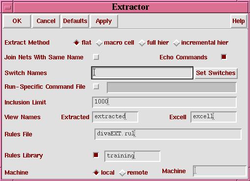
Extract Method: flat(階層展開モード)の選択
Switch Names: 今回は特に指定しない
View Names: Extracted: extracted, Excell: excell
Rule File: divaEXT.rul
Rules Library: training
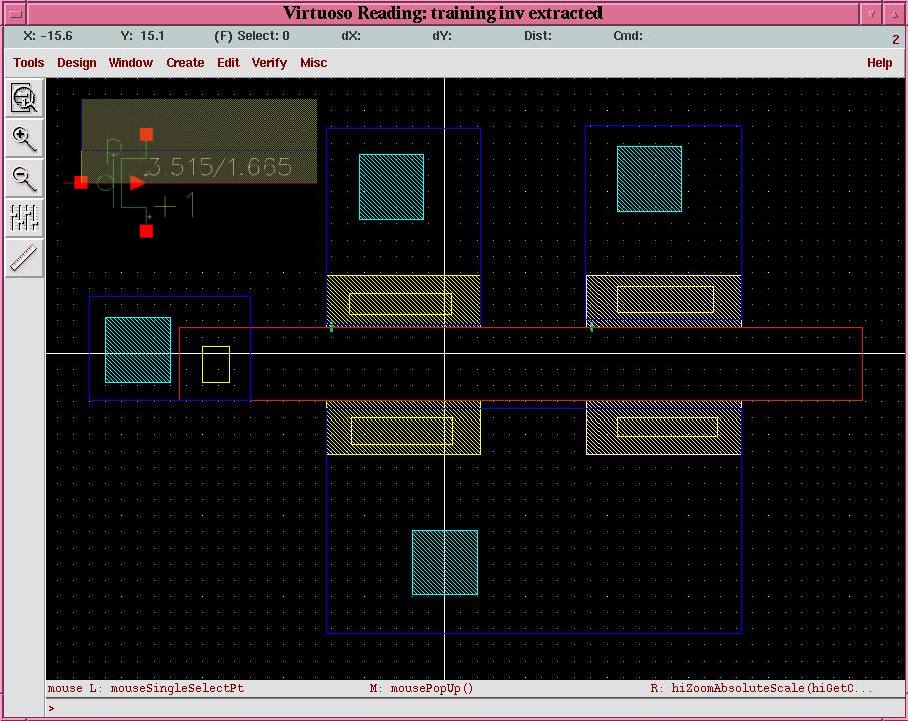
- 抽出図面の確認(Design > Load)
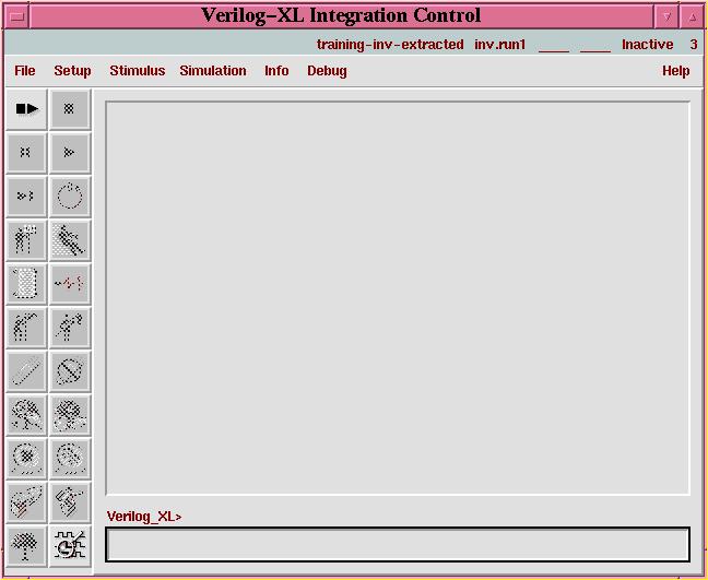
- シミュレーションモードへの移行(Tools > Verilog-XL)
Run Directory: 適宜入力(デフォルトは inv.run?) Library: training View: extracted としてしてOK 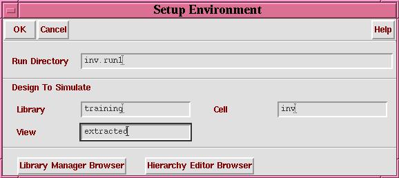
- Verilog-XL統合環境
- 回路抽出の際のオプション設定(Setup > Netlist)
More >> を押す 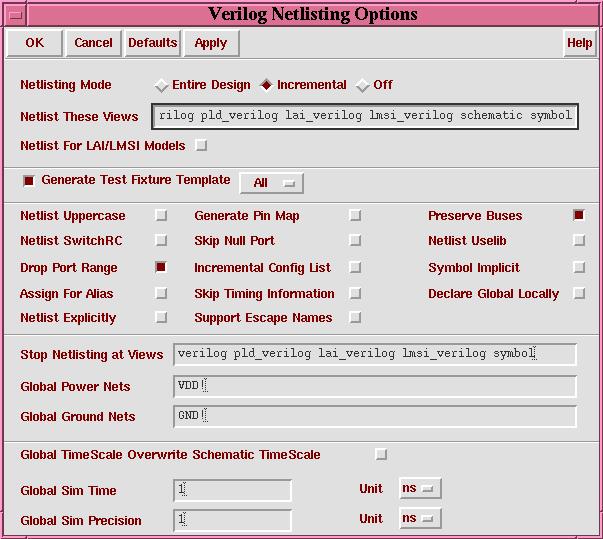
Netlisting Mode Entire Design Generate Test Fixture Template (ALL) Declare Global Locally Global Time Scale Overwrite Schematic Time Scale を選択してOK - STLによるシミュレーション入力ファイルの記述(Stimulus > STL > Edit STL Stimulus)
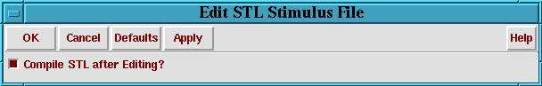
Compile STL after Editing? をチェックして OKをクリック
エディタでSTLのファイルを編集(XV行に時系列の1/0信号値を定義する); ---STL Source Program Template--- stlinit ; note that clock inputs should be of type "clk" defpin I in defpin "gnd!" in defpin "vdd!" in defpin O out deftiming 1e-09 1e-08 1e-07 ; define basic time units ; define any clocks or timing (defclock, defstrobe) ; define a basic format statement consisting of all the ; input and bidirectional nodes defformat "gnd!" "vdd!" I O ; if you wish to include both input and output nodes in the ; vectors, uncomment the following defformat statement ; defformat "gnd!" "vdd!" I gnd! vdd! O deftest ; define simulation stimulus values using xv command ; use binary truth table data, in the order of the ; defpin commands entered above. ; The following is an instance of a stimulus vector xv(0 1 0 ?) xv(0 1 1 ?) xv(0 1 1 ?) xv(0 1 0 ?) xv(0 1 1 ?) xv(0 1 0 ?) xv(0 1 1 ?) ; if you wish to define a vector with stimulus and ; expected output data use a vector of the following type ; xv(0 0 0 0 0 ?) endtest
- シミュレーションの実行(Simulation > Start Interactive, Simulation > Continue)
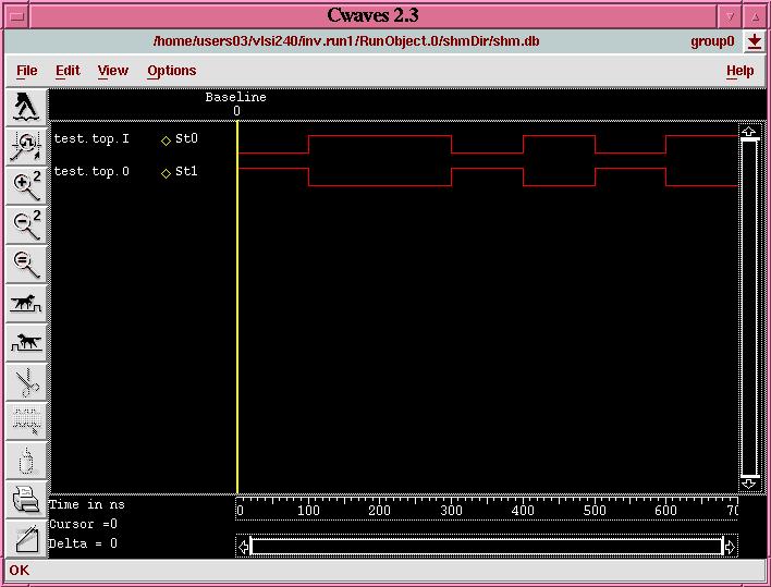
- 波形の観察(Debug > Utilities > View Waveform)
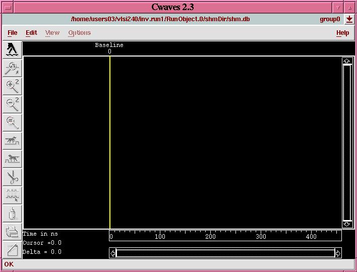
Edit > Browser/Display Toolを用いて信号を表示し動作を確認する 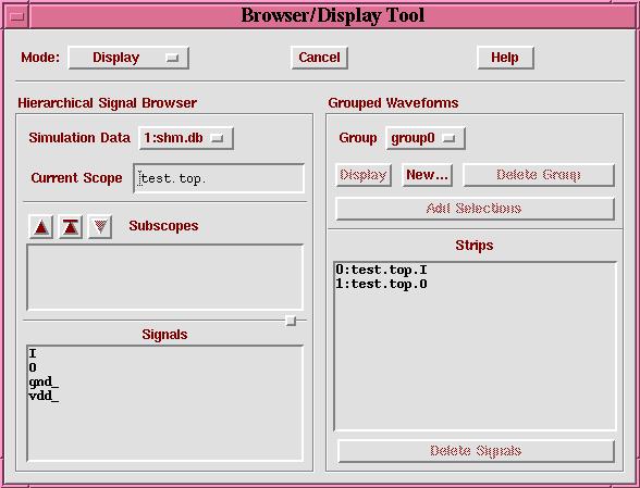
- STLによるシミュレーション入力ファイルの記述(Stimulus > STL > Edit STL Stimulus)