The 9th VDEC D2T Symposium
Presentation abstract

Close this window

Session 1 - Presentation 1
Title: Phase Noise and Jitter in Circuits: Origins, and How They Affect Signals
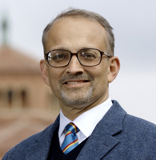
Speaker: Asad A. Abidi (University of California, Los Angeles)
Abstract:
Phase noise and jitter pose limits to resolution in communication receivers and measurement systems. This paper will show in simple ways the mechanisms that convert thermal noise in oscillators and amplifiers to fluctuations in time, and design methods for their mitigation.
It will also describe how to evaluate deterioration in the quality of various types of waveforms caused by mixing or sampling with clocks that are corrupted by jitter or phase noise.
Biography:
Asad A. Abidi received the B.Sc. (with Honors) degree from Imperial College, London, U.K. in 1976, and the M.S. and Ph.D. degrees in electrical engineering from the University of California, Berkeley, in 1978 and 1981, respectively.
He was at Bell Laboratories, Murray Hill, NJ, from 1981 to 1984 as a Member of Technical Staff in the Advanced LSI Development Laboratory. Since 1985, he has been with the Electrical Engineering Department of the University of California, Los Angeles, where he is Professor. He was a Visiting Faculty Researcher at Hewlett Packard Laboratories in 1989. His research interests are in CMOS RF design, data high-speed analog integrated circuit design, conversion, and other techniques of analog signal processing.
Dr. Abidi was the Program Secretary for the International Solid-State Circuits Conference from 1984 to 1990, and General Chairman of the Symposium on VLSI Circuits in 1992. He was Secretary of the IEEE Solid-state Circuits Council from 1990 to 1991. From 1992 to 1995, he was Editor of the IEEE Journal of Solid-state Circuits.

Session 1 - Presentation 2
Title: Numerical and Theoretical Analysis on Voltage and Time Domain Dynamic Range of Scaled CMOS Circuits
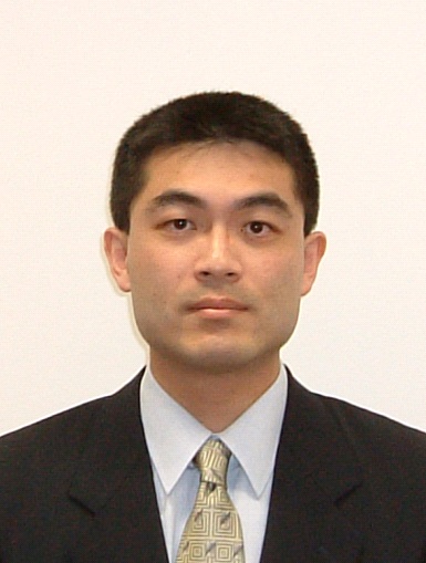
Speaker: Toru Nakura (The University of Tokyo)
Abstract:
It is believed that the time-domain resolution of a digital signal edge transition is superior to the voltage resolution of an analog signal in advanced CMOS processes. The reasoning behind this is that operating voltage has been reducing, making the signal more vulnerable to noise power due to scaling. On the other hand, in time domain, scaling has resulted to increase in frequency and therefore design of faster circuits, while also contributing to reduction of jitter. However, this is a concept that has not yet been quantitatively examined. This paper aims at verifying the effectiveness of the time-domain circuits over voltage-domain circuits in terms of their dynamic range performances by simulations as well as by theoretical analysis, especially in the scaled nano-meter processes. It has been shown that for a given technology the time domain dynamic range is superior to the voltage domain dynamic range by a factor of (ωT/B)^2 where ωT is the unity gain frequency and B is the bandwidth.
Biography:
Toru Nakura was born in Fukuoka, Japan in 1972. He received the B.S., M.S. and Ph.D. degree in electronic engineering from the University of Tokyo, Tokyo, Japan, in 1995, 1997 and 2005 respectively.
He has worked for industry as a circuit designer as well as an EDA tool developer, then he is currently an associate professor at VDEC (VLSI Design and Education Center) in the University of Tokyo. His research interest includes signal integrity and reliabllity of VLSI design.

Session 1 - Presentation 3
Title: A Subsampling Stochastic Coarse-Fine ADC with SNR 55.3dB and >5.8TS/s Effective Sample Rate for an on-Chip Signal Analyzer
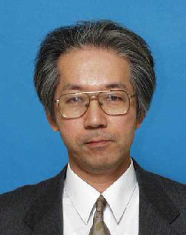
Speaker: Takahiro J. Yamaguchi (Advantest Laboratories)
Abstract:
In this presentation, we analyze the effect of nonlinear distortion, which is associated with comparator trip points, on the A/D conversion of a waveform using a stochastic analog-to-digital converter (ADC). It is demonstrated that reduction of the harmonic distortions along with a flat quantization noise spectrum can be realized in A/D conversions using a stochastic coarse-fine ADC.
Biography:
Takahiro J. Yamaguchi received the B.S. degree in applied physics from Fukui University, Fukui, Japan, in 1976, and the M.S. degree in physics, and Ph.D. degree in electronic engineering from Tohoku University, Sendai, Japan, in 1978, and 1999 respectively.
He joined Advantest Corporation in 1978, where he was a Research and Development Project Manager for Fourier analyzers, FFT-based servo analyzers, Michelson-type optical spectrum analyzers, and TV signal analyzers. Since 1991, he has been with Advantest Laboratories Ltd., Miyagi, Japan. Since 2009, he is also a researcher at VDEC, the University Tokyo. Presently he is a visiting professor at Gunma University, Gunma, Japan.
Dr. Yamaguchi and his group has presented 14 papers at ITC from year 2000, 8 papers at ISSCC, CICC, RFIC, A-SSCC, ISCAS and 6 journal papers.
He was a co-recipient of the DesignCon 2007 Best Paper, and the Honorable Mention Award at ITC2010 for ITC2009 jitter separation paper.

Session 2 - Presentation 1
Title: Present Status of Characteristics Variability in Advanced MOSFETs
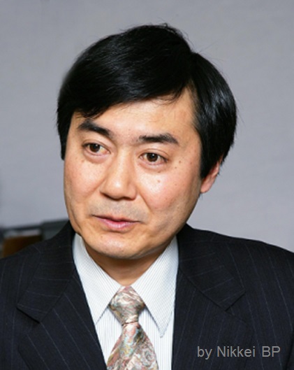
Speaker: Toshiro Hiramoto (The University of Tokyo)
Abstract:
The random variability of device characteristics is one of the most critical issues for further scaling of MOS transistors and further lowering of the supply voltage (Vdd). It has been recognized that the major origin of random Vth variability in bulk transistors is random dopant fluctuations (RDF). Due to increasing variability, some logic circuits or SRAM cells fail especially at low Vdd, resulting in severe yield loss. In order to deal with the variability problem, the extensive measurement, cause analysis, and developments of new suppression methods of variability are essential. In this presentation, the recent research activities on random variability measurements and variability suppression approaches are presented. In particular, the Vth measurement results of 11 billion bulk transistors and the random variability measurements of intrinsic channel FD SOI transistors and SRAM cells will be presented.
Biography:
Toshiro Hiramoto received B.S., M.S., and Ph.D degrees in electronic engineering from the University of Tokyo in 1984, 1986, and 1989, respectively. In 1989, he joined Device Development Center, Hitachi Ltd., Ome, Japan. He joined Institute of Industrial Science, University of Tokyo, Japan, in 1994 and he has been a Professor since 2002. His research interests include low power CMOS device design, variability in scaled transistors, silicon nanowire transistors, and silicon single electron transistors. Dr. Hiramoto is a fellow of Japan Society of Applied Physics and a member of IEEE and IEICE. He served as the General Chair of Silicon Nanoelectronics Workshop in 2003 and the Program Chair in 1997, 1999, and 2001. He was on Committee of IEDM from 2003 to 2009. He was the Program Chair of Symposium on VLSI Technology in 2013 and will be the General Chair in 2015.

Session 2 - Presenation 2
Title: Process and Design Differentiations at Ultra-Low-Voltage in UTBB FDSOI 28nm
Speaker: Philippe Roche (ST Microelectronics)
Abstract:
Electronics is more and more pervasive in everyday life (smartphones, connected cars, Internet-of-Things, wearable devices c) while energy constrained devices and harvesting technologies are progressively emerging. A major opportunity to dramatically reduce the energy consumption of digital circuits is to scale the supply voltage below 0.4V, driving them to the near-threshold regime. The idea of exploiting the weak-inversion operation of transistors for low power circuits was pioneered in the 60fs by Dr. Vittoz, applied to Swiss clocks, and is leading 50 years later to new exciting opportunities for sensor networks, medical electronics, wearable and multimedia devices. In this context, UTBB (Ultra-Thin Body and BOX) FD-SOI (Fully Depleted Silicon On Insulator) can be seen as a planar semiconductor technology particularly well suited for Ultra-Low-Voltage (ULV), thus ultra-low-power applications. Original ULV design solutions can also be used to leverage the low-power process capabilities while ensuring both performance and resilience below 0.6V. This talk will highlight the intrinsic capabilities of UTBB FDSOI near the threshold and present new design solutions down to 0.4V for logic cells, memories and CAD implementation. Circuit demonstrators, including 32 bits DSP, SPARCV8 and ARM cores, will also be reported with silicon test results below 0.35V in UTBB FDSOI 28nm.
Biography:
Dr. Philippe Roche received the M.S. (1995) and Ph.D. (1999) in Semiconductor Physics from Montpellier University, France. He consecutively worked at the US Radiation Lab., Vanderbilt University, Nashville, the Dutch 1/f Noise Lab., Eindhoven University, and French Atomic Commission, Military Applications, Bruy?res-le-Ch?tel. Since 1999, he has been with STMicroelectronics, Central R&D, Crolles, France, acting now as Fellow and Team Manager. He is in charge of radiation, safety aspects and sub-threshold (<0.4V) designs, intended to automotive, space, networking, medical and defence markets. His primary research activities are radiations effects, safety, as well as Ultra-Low-Voltage circuits from 350nm CMOS down to FDSOI 28/14nm. Philippe has also been driving the development of the new European Space technology in 65nm CMOS, as well as multiple IP upgrades for automotive platforms (ISO26262 compliant) in 55/40/28nm CMOS. He has been serving in conferences since 1997, as reviewer, session chairman and short course instructor, such as at IRPS, NSREC, IOLTS, DATE, RADECS, SOI and IEDM conferences. Philippe has co-authored 170+ papers, 6 book chapters and filed 50+ patents in radiation-hardening, safety and sub-threshold circuits.

Session 2 - Presenation 3
Title: Ultralow-Voltage Design and Technology of Silicon-on-Thin-Buried-Oxide (SOTB) CMOS for Highly Energy Efficient Electronics in IoT Era
Speaker: Nobuyuki Sugii (Low-power Electronics Association & Project)
Abstract:
Ultralow-voltage (ULV) operation of CMOS circuits is effective for significantly reducing the power consumption of the circuits. Although the operation at the minimum energy point (MEP) is effective, its slow operating speed has been an issue. The silicon-on-thin-buried-oxide (SOTB) CMOS is a strong candidate for the ultralow-power (ULP) electronics because of its small variability and back-bias control. These advantages of SOTB enable a power and performance optimization with adaptive Vth control at ULV and can achieve the ULP operation with acceptably high speed and low leakage. This paper describes our recent results on the ULV operation of CPU, SRAM, ring oscillator and other logic circuits. Our 32-bit RISC CPU chip named "Perpetuum Mobile" has a record low energy consumption of 13.4 pJ operating at 0.35 V and 14 MHz. This "Perpetuum-Mobile" micro-controllers are expected to be a core building block in a huge number of electronic devices in the internet-of-things (IoT) era.
Biography:
Nobuyuki Sugii (IEEE M'08) received the B.S., M.S., and Ph.D. degrees from the University of Tokyo. He joined the Central Research Laboratory, Hitachi, Ltd. in 1988. Currently, he leads the SOTB (Silicon on Thin Buried Oxide) research group in the Low-power Electronics Device Association & Project (LEAP). He is a member of the program committees of VLSI Technology, IEEE S3S Conference and SSDM. Since 2004, he also serves as a visiting professor for the Tokyo Institute of Technology.

Session 3 - Presentation 1
Title: Cross-Layer Approaches for Variation-aware System Design
Speaker: Mehdi B. Tahoori (Karlsruhe Institute of Technology)
Abstract:
As the minimum feature size continues to shrink, a host of vulnerabilities influence resiliency of VLSI circuits, such as increased process variation as well as runtime variations due to voltage and temperature fluctuations together with transistor and interconnect aging. Current approaches for robust circuit design consider only a small subset of these factors and typically address each of them in isolation. As a result, an over-pessimistic additive design margin, resulting from these sources, is eroding gains from technology scaling. In this talk I will discuss approaches to take into account netlist, layout and workload to capture all spatial and temporal information, and also consider the interplay of various process and runtime variation effects.
Biography:
Mehdi Tahoori, is professor and Chair of Dependable Nano-Computing (CDNC) at Karlsruhe Institute of Technology (KIT) in Germany since 2009. Before that he was an associate professor of ECE at Northeastern University, Boston, USA. He received his Ph.D. and M.S. in Electrical Engineering from Stanford University in 2003 and 2002, respectively. He has published close to 200 conference and journal papers on various aspects of robust system design and emerging technologies for computing. He has been on the organizing and technical program committee of various design automation, test, and dependability conferences. He is an associate editor of ACM Journal of Emerging Technologies for Computing. He was the recipient of National Science Foundation CAREER Award.

Session 3 - Presentation 2
Title: 30-Gb/s Optical and Electrical Test Solution for High-Volume Testing
Speaker: Daisuke Watanabe (Advantest Corporation)
Abstract:
To achieve high-volume testing of LSIs with high-speed optical and electrical interfaces, we developed a concept model of an optical LSI test system for mass-production. Key technologies include high-density and high-performance optical functional devices and a device interface that is capable of simultaneous connection of optical and electrical interfaces. Our proposed system enables the performance of multi-channel optical BER tests speeds of up to 30 Gb/s in several seconds by using PLZT thin-film modulators with results that correlate reasonably well with those measured by conventional BERTS. Moreover, our newly-developed opto-electronic hybrid test socket may permit high-volume testing with allowable insertion losses and repeatability. Additionally, our flexible system architecture can be applicable to testing at various laser wavelengths and with various optical parameters of optical LSI in combination with external instruments for optical characterization needs.
Biography:
Daisuke Watanabe was born in Kanagawa, Japan, on 1975. He received the B.E and M.E. degree in applied electronics from Tokyo University of Science, Japan in 1998 and 2000. In 2000, he joined Advantest Corporation, Gunma, Japan. Where he engaged in the R&D of ATE (Automatic Test Equipment) hardware.

Panel discussion
Theme: FD SOI for analog-digital compatibility in ultra-low voltage era
Moderator: Toshiro Hiramoto (The University of Tokyo)
Panelists: Asad A. Abidi (University of California, Los Angeles), Philippe Roche (ST Microelectronics), Nobuyuki Sugii (Low-power Electronics Association & Project), Mehdi B. Tahoori (Karlsruhe Institute of Technology)


VLSI Design and Education Center (VDEC), The University of Tokyo