The 11th VDEC D2T Symposium
Presentation abstract

Close this window

Session 1 - Presentation 1
Title: Design and Test of Micro-Electrode-Dot-Array (MEDA) Digital Microfluidic Biochips
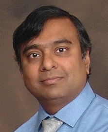
Speaker: Krishnendu Chakrabarty (Duke University & VDEC, The University of Tokyo)
Abstract:
A digital microfluidic biochip (DMFB) is an attractive technology platform for automating laboratory procedures in biochemistry. However, today's DMFBs suffer from several limitations: (i) constraints on droplet size and the inability to vary droplet volume in a fine-grained manner; (ii) the lack of integrated sensors for real-time detection; (iii) the need for special fabrication processes and reliability/yield concerns. To overcome the above problems, DMFBs based on a micro-electrode-dot-array (MEDA) architecture, and fabricated using a TSMC 350 nm process, have recently been demonstrated.
This presentation will first describe a biochemistry synthesis approach for such MEDA biochips. This synthesis method targets operation scheduling, module placement, routing of droplets of various sizes, and diagonal movement of droplets in a two-dimensional array. Simulation results using benchmarks and experimental results using a fabricated MEDA biochip will be presented to demonstrate the effectiveness of the proposed co-optimization technique. Finally, the presentation will describe an efficient built-in self-test (BIST) solution for MEDA biochips. Simulation results based on HSPICE and experiments using fabricated MEDA biochips will highlight the effectiveness of the proposed BIST architecture.
Biography:
Krishnendu Chakrabarty received the B. Tech. degree from the Indian Institute of Technology, Kharagpur, in 1990, and the M.S.E. and Ph.D. degrees from the University of Michigan, Ann Arbor, in 1992 and 1995, respectively. He is now the William H. Younger Distinguished Professor of Engineering in the Department of Electrical and Computer Engineering and Professor of Computer Science at Duke University. He also serves as Director of Graduate Studies for Electrical and Computer Engineering. Prof. Chakrabarty is a recipient of the National Science Foundation Early Faculty (CAREER) award, the Office of Naval Research Young Investigator award, the Humboldt Research Award from the Alexander von Humboldt Foundation, Germany, the IEEE Transactions on CAD Donald O. Pederson Best Paper award (2015), and 11 best paper awards at major IEEE conferences. He is also a recipient of the IEEE Computer Society Technical Achievement Award (2015) and the Distinguished Alumnus Award from the Indian Institute of Technology, Kharagpur (2014). He is a Research Ambassador of the University of Bremen (Germany) and a Hans Fischer Senior Fellow (named after Nobel Laureate Prof. Hans Fischer) at the Institute for Advanced Studies, Technical University of Munich, Germany.
Prof. Chakrabarty's current research projects include: testing and design-for-testability of integrated circuits; digital microfluidics, biochips, and cyberphysical systems; optimization of enterprise systems and smart manufacturing. Prof. Chakrabarty is a Fellow of ACM, a Fellow of IEEE, and a Golden Core Member of the IEEE Computer Society. He holds eight US patents, with several patents pending. He was a 2009 Invitational Fellow of the Japan Society for the Promotion of Science (JSPS). He is a recipient of the 2008 Duke University Graduate School Dean's Award for excellence in mentoring, and the 2010 Capers and Marion McDonald Award for Excellence in Mentoring and Advising, Pratt School of Engineering, Duke University. He has served as a Distinguished Visitor of the IEEE Computer Society (2005-2007, 2010-2012), and as a Distinguished Lecturer of the IEEE Circuits and Systems Society (2006-2007, 2012-2013). Currently he serves as an ACM Distinguished Speaker.
Prof. Chakrabarty served as the Editor-in-Chief of IEEE Design & Test of Computers during 2010-2012 and ACM Journal on Emerging Technologies in Computing Systems during 2010-2015. Currently he serves as the Editor-in-Chief of IEEE Transactions on VLSI Systems. He is also an Associate Editor of IEEE Transactions on Computers, IEEE Transactions on Biomedical Circuits and Systems, IEEE Transactions on Multiscale Computing Systems, and ACM Transactions on Design Automation of Electronic Systems. He serves as an Editor of the Journal of Electronic Testing: Theory and Applications (JETTA). In the recent past, he has served as Associate Editor of IEEE Transactions on VLSI Systems (2005-2009), IEEE Transactions on Computer-Aided Design of Integrated Circuits and Systems (2001-2013), IEEE Transactions on Circuits and Systems I (2005-2006), and IEEE Transactions on Circuits and Systems II (2010-2013).

Session 1 - Presentation 2
Title: IMPACT: Implantable Microsystems for Personalised Anti-Cancer Therapy
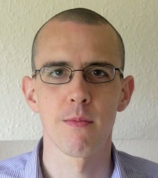
Speaker: Stewart Smith (Edinburgh University & VDEC, The University of Tokyo)
Abstract:
IMPACT aims to develop new approaches to cancer treatment using implanted miniaturised, wireless sensor chips the size of a grass seed to monitor the minute-to-minute status of an individual tumour. The project brings together engineers, chemists, veterinary clinicians, social scientists and human cancer specialists from the University of Edinburgh, Heriot-Watt University and the Western General Hospital. This multi-disciplinary group is led by Prof Alan Murray from the University of Edinburgh's School of Engineering. In this presentation, Dr Stewart Smith, will introduce the aims of the IMPACT project and explain the work involved in miniaturising and integrating electrochemical sensors to measure key biomarkers of cancerous tumours. These involve post processing of foundry CMOS electronics and the integration of biosensing materials, as well as the challenges of packaging microelectronic systems for the adverse environment within the human body.
Biography:
Stewart Smith received the B.Eng.(hons) degree in electronics and electrical engineering in 1997 and the Ph.D. degree in 2003 from the University of Edinburgh, Scotland, UK. He is currently a lecturer in the School of Engineering at the University of Edinburgh and a member of the Research Institute for Bioengineering. Stewart is a member of the Royal Society of Edinburgh, Young Academy of Scotland and the technical committee for the IEEE International Conference on Microelectronic Test Structures. His current research interests include the design and fabrication of bioelectronic and biomedical microsystems, microfluidics and biosensors, and development of test structures for MEMS and microsystems processes.

Session 2 - Presenation 1
Title: Experimental Demonstration of Cancelling Systematic Variation for free-Calibration Stochastic ADC
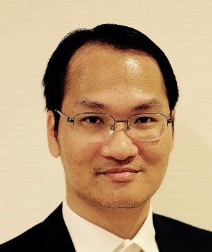
Speaker: Nguyen Ngoc Mai-Khanh (VDEC, The University of Tokyo)
Abstract:
Instead of suppressing process variations, stochastic analog-to-digital converter (ADC) utilizes them to build a multi-Gaussian transfer function based on a number of stochastic comparators. The transfer function or cumulative distribution function (CDF) comprises of all comparator elements' offset distributions and the limited linear region neighboring to the CDF's trip point is used. Two factors, systematic and random variations, contribute to the stochastic ADC's CDF; however, the former should be excluded for the purpose of stochastic ADC operation.
In this presentation, we present an experimental demonstration of cancelling systematic variance for free-calibration stochastic ADC. A layout strategy is presented for the purpose of cancelling systematic variation and to obtain Gaussian offset distribution with a reasonable number of comparators. Measurement data of four chips fabricated in a 180-nm CMOS process with a low noise fully differential measurement setup shows an effective LSB resolution smaller 10 times than that of the conventional approach but with the number of comparators less than 10 times. The demonstration on the relationship of number of comparators and the effective resolution LSB of stochastic ADC is helpful for a design-guide for the trade-off between the number of comparator elements, required LSB resolution, die area, and power consumption for fine-resolution stochastic ADC approach.
Biography:
Nguyen Ngoc Mai-Khanh received the B.S. and M.S. degrees in Electrical Engineering from the University of Technology, National University, Vietnam, in 2002 and 2004, respectively, and Ph.D. degree in Electrical Engineering and Information Systems, the University of Tokyo, Japan in 2011. During January 2006 to June 2006, he joined a short-term project for the internship in Toshiba R&D, Kawasaki, Japan. He was a lecturer of Faculty of Electrical and Electronic Engineering, the University of Technology, National University, Viet Nam from 2006 to 2013.
Dr. Mai-Khanh worked as a post-doctoral researcher in VLSI Design and Education Center (VDEC), the University of Tokyo, Japan from 2011 to 2013 and currently is an Assistant Professor at VDEC.
His research interests include integrated analog circuits, magnetic sensors and applications, and mm-wave wideband integrated transceiver. He received the Best Paper Award of the Asian Symposium on Quality Electronic Design 2010 Symposium and the third rank of the Best Student Paper Award of the 9th IEEE NEWCAS 2011. Dr. Mai-Khanh has served as a reviewer on IEEE Journal of Sensor, IEEE Microwave and Wireless Components Letters, Springer Journal of Analog Integrated Circuits and Signal Processing, IEEE NEWCAS conference, IEEE Sensor Application Symposium, and Advanced Technologies for Communications (ATC) conference.

Session 2 - Presenation 2
Title: A new method for measuring alias-free aperture jitter in an ADC output
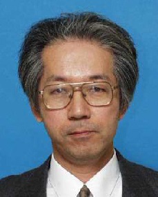
Speaker: Takahiro J. Yamaguchi (Advantest Laboratories Ltd.)
Abstract:
This paper proposes a new method for directly measuring alias-free aperture jitter in an ADC output. Both the average ENOB and the worst-case ENOB due to aperture jitter are also measured after the elimination of the aliasing noise. Because it adds only a negligible computation time to an existing ENOB test of a single frequency, it can also be used in an HV production environment and should reduce the overall test time by at least three times.
Biography:
Takahiro J. Yamaguchi received the B.S. degree in applied physics from Fukui University, Fukui, Japan, in 1976, and the M.S. degree in physics, and Ph.D. degree in electronic engineering from Tohoku University, Sendai, Japan, in 1978, and 1999 respectively.
He joined Advantest Corporation in 1978, where he was a Research and Development Project Manager for Fourier analyzers, FFT-based servo analyzers, Michelson-type optical spectrum analyzers, and TV signal analyzers. Since 1991, he has been with Advantest Laboratories Ltd., Miyagi, Japan. Since 2009, he is also a researcher at VDEC, the University Tokyo. From 2009 to 2014, he was a visiting professor at Gunma University, Gunma, Japan.
Dr. Yamaguchi and his group has presented 14 papers at ITC from year 2000, 11 papers at ISSCC, VLSI CIRCUITS, CICC, RFIC, A-SSCC, ISCAS and 7 journal papers.
He was a co-recipient of the DesignCon2007 Best Paper, and the Honorable Mention Award at ITC2010 for ITC2009 jitter separation paper. From 2010 to 2015, he served as a member of the Technical Program Committee of the IEEE Custom Integrated Circuits Conference (CICC).

Session 2 - Presenation 3
Title: Power Supply Impedance Emulation Technique for ATE Device Power Supply
Speaker: Masahiro Ishida (Advantest Corporation)
Abstract:
In this presentation, we proposes a new concept of power supply impedance emulation technique for automatic test equipment (ATE) device power supply that has ability to emulate an arbitrary power supply characteristic. It can emulate power supply impedance of customer environment so as to match the power supply voltage fluctuation waveforms of the ATE and of the customer environment, and hence eliminate overkills and underkills due to power supply characteristic difference between the ATE and a practical operating environment. Our technique adjusts the equivalent impedance by injecting compensation current by a current source attached in parallel with the power supply source. The compensation current is calculated and injected in real-time with a feedback manner based on the power supply voltage measurement with the impedance characteristics of ATE's original power delivery network (PDN) and the customer PDN.
Biography:
Masahiro Ishida received the B.S. and the M.S. degree in electronic and information engineering from Tokyo University of Agriculture and Technology, Japan, in 1993 and 1995, respectively, and the Ph.D. degree in engineering from the University of Tokyo, Japan, in 2013. He joined Advantest Laboratories Ltd. in 1995 and contributed to the development of jitter measurement method. From 2009, he worked for Advantest Corporation, Japan and developed a real-time functional testing method for the multi-level signal and the digital modulation signal interfaces. And since 2010, he has been doing a joint research on controlling and testing the power integrity of the device under test with the University of Tokyo. His current research interests include testing methods for signal integrity and power integrity.

Session 2 - Presenation 4
Title: High-throughput and high-accuracy electron-beam direct writing
Speaker: Rimon Ikeno (VDEC, The University of Tokyo)
Abstract:
The high throughput of character projection (CP) electron-beam (EB) lithography makes it a promising technique for low-to-medium volume device fabrication with regularly arranged layouts, such as for standard-cell logics and memory arrays. However, non-VLSI applications such as MEMS and MOEMS may not be able to fully utilize the benefits of the CP method due to the wide variety of layout figures including curved and oblique edges. In addition, the stepwise shapes that appear because of the EB exposure process often result in intolerable edge roughness, which degrades device performances. In this study, we propose a general EB lithography methodology for such applications utilizing a combination of the CP and variable-shaped beam methods. In the process of layout data conversion with CP character instantiation, several control parameters were optimized to minimize the shot count, improve the edge quality, and enhance the overall device performance. We have demonstrated EB shot reduction and edge-quality improvement with our methodology by using a leading-edge EB exposure tool, ADVANTEST F7000S-VD02, and a high-resolution hydrogen silsesquioxane resist. Atomic force microscope observations were used to analyze the resist edge profiles' quality to determine the influence of the control parameters used in the data conversion process.
Biography:
Rimon Ikeno received his B.S., M.S., and Ph.D. degrees in electronic engineering from the University of Tokyo in 1992, 1994, and 1997, respectively.
He joined Texas Instruments in 1997, and worked on advanced CMOS devices/process, ultra-low power circuit technology, and low-power DSP core development for mobile applications. After leaving TI in 2008, he worked at two Japanese venture companies for low-power and high-performance computing systems.
In 2011, he joined the University of Tokyo again, and currently, he is in charge of Advantest D2T research division in VDEC as a project lecturer. His research interests include advanced device/process technology, VLSI design methodology, VLSI testing, and low-power data processing systems.

Session 3 - Presentation 1
Title: Options for the integration of technologies with CMOS Integrated Circuits
Speaker: Anthony J. Walton (Edinburgh University)
Abstract:
CMOS integrated circuit technology continues to be scaled to smaller geometries as companies follows Moore`s predictions. With this scaling down of dimensions the cost associated with manufacturing ICs at sub 20nm technology has resulted in many companies being either unable, or unwilling, to justify such an investment. As a consequence many have decided to go fabless while others have diversified into new device types and more niche application areas.
One very attractive option for both IC producers and fabless companies to use a standard silicon as a platform for system integration. The added value associated with post-processing directly on top of the silicon circuitry can then be provided in-house by companies with the required technology or via third party providers for fabless operations. This presentation examines many of the issues associated with integrating foundry and custom IC wafers with both new materials and technologies such as MEMS based sensors and actuators. It discusses the options available for companies considering such applications and presents examples of successful implementations of a number of different approaches.
Biography:
Anthony J. Walton is professor of Microelectronic Manufacturing in the School of Engineering at the University of Edinburgh. Over the past 30 years his research has involved the fabrication of a wide variety sensors and micro-systems which also includes the integration of materials and processes on foundry silicon ICs. He has helped to pioneer the development of electrodes for high temperature (550 deg-C) operation in molten salts and nanoelectrode sensor arrays, and led the microsystems element in the fabrication of the world's most sensitive bolometer array (10-17 W/Hz) now operational on the James Clark Maxwell telescope in Hawaii. His present interests also include the applications of micro and nanotechnology to biotechnology, microelectronic test structures, and integrating new technologies (such as MEMS) and materials with foundry CMOS. He played a key role in setting up the Scottish Microelectronics Centre (SMC) which is a purpose built facility for R&D and incubation. It consists of approximately 300m2 of class 10 cleanrooms with a very comprehensive set of CMOS and MEMS equipment.
He has published over 400 papers and has won the best paper awards for the IEEE Transactions on Semiconductor Manufacturing, Proc. International Society for Hybrid Manufacturers (ISHM), the International Conference on Microelectronic Test Structures (ICMTS), the International Journal of Molecular Sciences as well as prizes at Nanotech 06 Lab on a Chip best paper award. (Montreux), IET Nanobiotechnology, IET Premium Paper Award. He is a Fellow of the Royal Society (Edinburgh) and has served as the chairman for a number of conferences which include the European Solid-State Devices Research Conference (ESSDERC/CIRC 1994 and 2008) and the IEEE International Conference on Microelectronic Test Structures (ICMTS 1989 and 2008). He also serves on numerous technical committees and is an associate editor of the IEEE Transactions on Semiconductor Manufacturing and the Journal of Nanoengineering and Nanosystems.

Session 3 - Presentation 2
Title: 3D Integrated CMOS-Memristor Hybrid Circuits: Devices, Integration, Architecture, and Applications
Speaker: Kwang-Ting (Tim) Cheng (Hong Kong University of Science and Technology)
Abstract:
I will give an overview of our recent research efforts on monolithic 3D integration of CMOS and memristive nanodevices. These hybrid circuits combine a CMOS subsystem with multiple layers of nanowire crossbars, consisting of arrays of two-terminal memristors, all connected by an area-distributed interface between the CMOS subsystem and the crossbars. Combining the advantages of CMOS technology with the extremely high density of memristors and interface vias, this approach could offer unprecedented memory density and bandwidth at manageable power dissipation, and enable new memory-centric computing paradigms. Specifically, I will highlight our results in four areas: (1) memristive device development and engineering which achieves better performance, endurance and uniformity, (2) 3D monolithic integration of CMOS with up to 8 layers of memristive crossbars, (3) architectures for building low-power, reliable resistive RAM (ReRAM), and (4) applications to bio-inspired mixed-signal computing.
Biography:
K.-T. Tim Cheng received his Ph.D. in EECS from the University of California, Berkeley in 1988. He worked at Bell Laboratories from 1988 to 1993 and was on the faculty at the University of California, Santa Barbara from 1993 to April 2016 where he was Professor of ECE and served as the founding director of UCSB's Computer Engineering Program (1999-2002), Chair of the ECE Department (2005-2008), and A ssociate Vice Chancellor for Research (2013-2016). He is currently with Hong Kong University of Science and Technology (HKUST), serving as Dean of Engineering and Chair Professor of ECE and CSE. His current research interests include design, automation and test for SoC/photonic IC/flexible electronics/3D hybrid circuits, mobile embedded systems and mobile computer vision. He has published more than 400 technical papers, co-authored five books, and holds 12 U.S. Patents in these areas. He recently served as the principle investigator for US Department of Defense MURI project for 3D hybrid circuits which aims at integrating CMOS with high-density memristors.
Cheng, an IEEE fellow, received 10+ Best Paper Awards from various IEEE conferences and journals. He has also received the UCSB College of Engineering Outstanding Teaching Faculty Award. He served as Editor-in-Chief of IEEE Design and Test of Computers (2006-2009) and was a board member of IEEE Council of Electronic Design Automation's Board of Governors, IEEE Computer Society's Publication Board, and working groups of International Technology Roadmap for Semiconductors (ITRS).

Panel discussion
Theme: Breakthrough technology and application of heterogeneous micro/nano systems for industrial/economic success
Moderator: Hiroyuki Fujita (Institute of Industrial Science, The University of Tokyo)
Biography:
Hiroyuki Fujita is Professor (1993-present) and served as the Deputy Director (2009-2012) of the Institute of Industrial Science (IIS), The University of Tokyo. He is also the Director of the Center for International Research on Micronano Mechatronics (2000-present). He received the B.S., M.S. and Ph.D. degrees from Department of Electrical Engineering of The University of Tokyo, Tokyo, Japan in 1975, 1977 and 1980, respectively. He joined IIS as an assistant professor just after earning his Ph.D. degree. Recently he stayed in UC Berkeley as a Russell Severance Springer Professor.
His research interest includes VLSI-compatible micro/nano fabrication, microactuators, and MEMS application to nano science and bio technology.
He received M. Hetenyi Award of Experimental Mechanics from the Society for Experimental Mechanics in 1986, Chevalier de l'Ordre des Palmes Academiques from Government of France in 2001, The Prize for Science and Technology in Research Category from Japanese Ministry of Education, Culture, Sports, Science and Technology in 2005, Outstanding Achievement Award from The Institute of Electrical Engineers of Japan in 2005, and The Yamazaki-Teiichi Prize from Foundation for Promotion of Material Science and Technology of Japan in 2013.
Panelists:
Anthony Walton (Edinburgh University)
Tim Cheng (Hong Kong University of Science and Technology)
Krishnendu Chakrabarty (Duke University & VDEC, The University of Tokyo)
Stewart Smith (Edinburgh University & VDEC, The University of Tokyo)


VLSI Design and Education Center (VDEC), The University of Tokyo