The 12th VDEC D2T Symposium
Presentation abstract

Close this window

Session 1 - Presentation 1
Title: Advanced MOS device technology for ultra-low power IoT applications
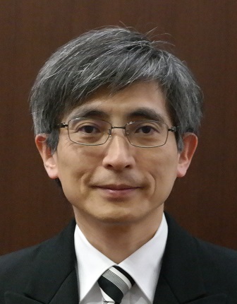
Speaker: Shinichi Takagi (The University of Tokyo)
Abstract:
Low power consumption is one of the most important requirements for present and future integrated systems, particularly IoT applications, some of which should be driven by battery with no need of replacement or energy harvesting power supply. Here, reduction in supply voltage is most effective in power reduction. Low supply voltage operation of charge-based logic switch devices can be achieved typically by two strategies. One is realization of higher Ion due to higher mobility or velocity channels. Since on-current under ballistic/quasi ballistic transport is proportional to injection velocity at source edge, low effective mass materials are preferred. From this viewpoint, III-V/Ge materials are promising. The other strategy is to develop steep slope devices with lower sub-threshold swing than CMOS. For this purpose, there are two directions, sensitivity increase in surface potential with respect to gate voltage change and introduction of a new carrier conduction mechanism. Examples of the former and the latter directions are negative gate capacitance MOSFETs and tunnel FETs (TFETs), respectively. Particularly, TFETs have recently stirred a strong interest, because of the high compatibility with CMOS platform. Here, materials with small and/or direct band gap such as III-V and Ge are preferred to enhance on-current of TFETs. In this presentation, the critical issues and difficult challenges of such ultra-low power MOS devices are addressed with an emphasis on Ge and III-V channels. Some of viable technologies and demonstrated devices on the Si CMOS platform are introduced for solving these problems.
Biography:
Shinichi Takagi was born in Tokyo, Japan, on August 25, 1959. He received the B.S., M.S. and Ph.D. degrees in electronic engineering from the University of Tokyo, Tokyo, Japan, in 1982, 1984 and 1987, respectively. His Ph.D. thesis involved the study on the surface carrier transport in MISFETs based on III-V semiconductors. He joined the Toshiba Research and Development Center, Kawasaki, Japan, in 1987, where he has been engaged in the research on the device physics of Si MOSFETs, including the carrier transport in the inversion layer, the impact ionization phenomena, the hot carrier degradation and the electric properties of Si/SiO2 interface. From 1993 to 1995, he was a Visiting Scholar at Stanford University, Stanford, CA, where he studied the Si/SiGe hetero-structure devices. Since returning to the ULSI Research Laboratories, he was also engaged in the physics and technology of the reliability of SiO2, ferroelectric devices and strained-Si MOS devices. He worked for the MIRAI Project as the leader of Ultra-High Performance New Transistor Structures Theme from 2001 to 2007. In October 2003, he moved to the University of Tokyo, where he is currently working as a professor in the department of Electrical Engineering and Information Systems, School of Engineering. His recent interests include the science and the technologies of advanced CMOS devices using new channel materials such as strained-Si, Ge and III-Vs.
Dr. Takagi served on the technical program committee on several international conferences including International Electron Device Meeting, Symposium on VLSI Technology, International Reliability Physics Symposium, International Conference on Solid State Device and Materials and International Solid State Circuits Conference. He is a member of the IEEE Electron Device Society and the Japan Society of Applied Physics.

Session 1 - Presentation 2
Title: Going Digital: Transformation of Society, Industry, and Life
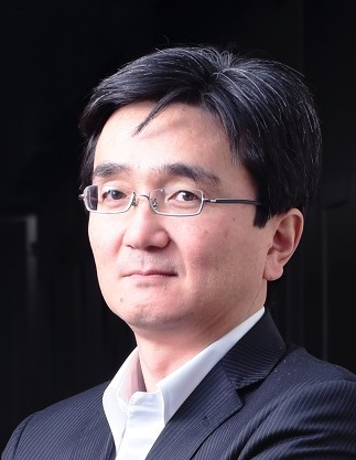
Speaker: Hiroyuki Morikawa (The University of Tokyo)
Abstract:
Data forms a key pillar in 21st century sources of growth. OECD is discussing the value of data as a new source of growth. The large data sets are becoming a core asset in the economy, fostering new industries, processes and products and creating significant competitive advantages. Big Data, IoT (Internet of Things), and M2M (Machine-to-machine) will be the key for realizing designing a future.
Peter Drucker investigated the impact of railroad on society. "The technology of the steam engine did not end with the railroad." Although gthe railroad made the Industrial Revolution accomplished fasth, the boom it triggered lasted almost a hundred years. The dynamics of the technology shifted to totally new "social institutions: the modern postal service, the daily paper, investment banking, and commercial banking, to name just a few."
Information and communication technology has also had an enormous impact on society. However, the information and communication technology did not end with broadband infrastructure as Peter Drucker revealed in the case of railroad. The most important impact of the technology should be the creation of totally new industries such as postal service, daily paper, and banking.
The talk begins with the value of data. The effect of data to our society is shown to be similar to that of PLC (Programmable Logic Controller). Digitalization promotes the re-definition of business and R&D in all industrial segments, and increases productivity and creates value. Next, the value of data is shown in the area of health care, social infrastructure, agriculture, city planning, and maintenance. Finally, the directions and challenges for realizing data-driven economy are identified for designing a future from the viewpoints of digitalization of physical assets, general purpose technology, re-definition of business and organization, importance of "marines" type units, and the difference between invention and innovation.
Biography:
Hiroyuki Morikawa received the B.E., M.E, and Dr. Eng. degrees in electrical engineering from the University of Tokyo, Tokyo, Japan, in 1987, 1989, and 1992, respectively. Since 1992, he had been in the University of Tokyo and is currently a full professor of School of Engineering at the University of Tokyo. From 2002 to 2006, he was a group leader of the NICT Mobile Networking Group. His research interests are in the areas of ubiquitous networks, sensor networks, big data/IoT/M2M, wireless communications, and network services. He served as a technical program committee chair of many IEEE/ACM conferences and workshops, Vice President of IEICE, Editor-in-Chief of IEICE Transactions of Communications, OECD Committee on Digital Economy Policy (CDEP) vice chair, Director of New Generation M2M Consortium, and he sits on numerous telecommunications advisory committees and frequently serves as a consultant to government and companies. He has received more than 50 awards including the IEICE best paper award in 2002, 2004, and 2010, the IPSJ best paper award in 2006, JSCICR best paper award in 2015, the Info-Communications Promotion Month Council President Prize in 2008, the NTT DoCoMo Mobile Science Award in 2009, the Rinzaburo Shida Award in 2010, and the Radio Day Ministerial Commendation in 2014.

Session 2 - Presenation 1
Title: Power Supply Impedance Emulation to Eliminate Overkills and Underkills due to the Impedance Difference between ATE and Customer Board
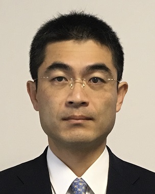
Speaker: Toru Nakura (The University of Tokyo)
Abstract:
This paper proposes a new type of power supply circuit for automatic test equipment (ATE) that has ability to emulate arbitrary power supply impedance. It can emulate power supply impedance of customer environment so as to match the power supply voltage fluctuation waveforms of the ATE and of the customer environment, in order to eliminate overkills/underkills coming from the voltage fluctuation difference caused by the impedance difference between the ATE and a practical operating environment. Our technique adjusts the equivalent impedance by injecting compensation current by a current source attached in parallel with the power supply source. The compensation current is calculated and injected in realtime with a feedback manner based on the power supply voltage measurement with the impedance characteristics of ATEfs original power delivery network (PDN) and the customer PDN. Experimental results of prototype circuits are demonstrated to show that the compensation current emulates the impedance, and the both power supply voltage fluctuation waveforms agree well. Limitations and applications of our method are also discussed.
Biography:
Toru Nakura was born in Fukuoka, Japan in 1972. He received the B. S., and M. S. degree in electronic engineering from The University of Tokyo, Tokyo, Japan, in 1995 and 1997 respectively. Then he worked as a circuit designer of high-speed communication using SOI devices for two years, and worked as a EDA tool developer for three years. He joined the University of Tokyo again as a Ph.D student in 2002, and received the degree in 2005. After two years industrial working period, he is back to academia as an associate professor at VLSI Design and Education Center (VDEC), The University of Tokyo. He is now currently working as an associate professor in the department of Electrical Engineering and Information Systems in the University of Tokyo. His current interest includes signal integrity, reliability, power supply, digitally-assist analog circuits, and fully automated analog circuit synthesis.

Session 2 - Presenation 2
Title: Common Pitfalls in Application of a Threshold Detection Comparator to a Continuous-Time Level Crossing Quantization
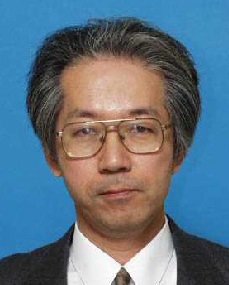
Speaker: Takahiro J. Yamaguchi (Advantest Laboratories Ltd.)
Abstract:
Propagation delay variation of the threshold detection comparator in current-day level-crossing ADCs is a fundamental impediment to their performance. This paper reviews why commonly used threshold detection comparators can be inappropriate to detect level crossing times of high-frequency signals. The analysis presented in this paper helps establish a new common ground for developing a high-performance LCADC.
Biography:
Takahiro J. Yamaguchi received the B.S. degree in applied physics from Fukui University, Fukui, Japan, in 1976, and the M.S. degree in physics, and Ph.D. degree in electronic engineering from Tohoku University, Sendai, Japan, in 1978, and 1999 respectively.
He joined Advantest Corporation in 1978, where he was a Research and Development Project Manager for Fourier analyzers, FFT-based servo analyzers, Michelson-type optical spectrum analyzers, and TV signal analyzers. Since 1991, he has been with Advantest Laboratories Ltd., Miyagi, Japan. Since 2009, he is also a researcher at VDEC, the University Tokyo. From 2009 to 2014, he was a visiting professor at Gunma University, Gunma, Japan.
Dr. Yamaguchi and his group has presented 14 papers at ITC from year 2000, 11 papers at ISSCC, VLSI CIRCUITS, CICC, RFIC, A-SSCC, ISCAS and 7 journal papers.
He was a co-recipient of the DesignCon2007 Best Paper, and the Honorable Mention Award at ITC2010 for ITC2009 jitter separation paper. From 2010 to 2015, he served as a member of the Technical Program Committee of the IEEE Custom Integrated Circuits Conference (CICC).

Session 3 - Presenation 1
Title: Variation and Failure Characterization Through Test Data Analytics
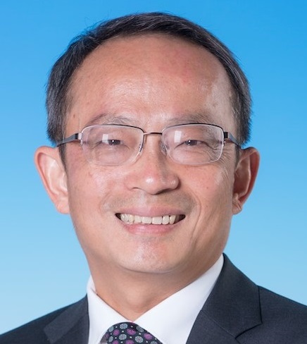
Speaker: Kwang-Ting Cheng (Hong Kong University of Science and Technology)
Abstract:
We describe a framework for characterizing systematic variations and failures through exploring the hidden patterns of test data from multiple test stages. The framework first provides prediction of process variations with a fine resolution based on a limited number of probed process parameters. An unsupervised biclustering technique is then utilized to extract spatial patterns from process parameters and production test results, respectively, through analyzing both item-to-item and die-to-die correlations in subsets of the test data. A template matching technique exploits these spatial patterns to discover connections between process variations and failures detected by production tests. The proposed framework has been verified by an industrial test dataset of a non-volatile memory product. The discovery of comprehensible correlations between process parameters and some production test items was confirmed by the engineers who have insights to the test dataset.
Biography:
Kwang-Ting (Tim) Cheng received his Ph.D. in EECS from the University of California, Berkeley in 1988. He has been serving as Dean of Engineering and Chair Professor of ECE and CSE at Hong Kong University of Science and Technology (HKUST) since May 2016. He worked at Bell Laboratories from 1988 to 1993 and joined the faculty at Univ. of California, Santa Barbara in 1993 where he was the founding director of UCSB's Computer Engineering Program (1999-2002), Chair of the ECE Department (2005-2008) and Associate Vice Chancellor for Research (2013-2016). His current research interests include hardware verification and security, design automation for photonics IC and flexible hybrid circuits, memristive memories, mobile embedded systems, and mobile computer vision. He has published more than 400 technical papers, co-authored five books, adviced 40+ PhD theses, and holds 12 U.S. Patents in these areas.
Cheng, an IEEE fellow, received 10+ Best Paper Awards from various IEEE and ACM conferences and journals. He has also received UCSB College of Engineering Outstanding Teaching Faculty Award. He served as Editor-in-Chief of IEEE Design and Test of Computers and was a board member of IEEE Council of Electronic Design Automation's Board of Governors and IEEE Computer Society's Publication Board.

Session 3 - Presenation 2
Title: Test Chip Design for Yield Learning in 7nm Semiconductor Technologies
Speaker: Shawn Blanton (Carnegie Mellon University)
Abstract:
It is common practice for design houses (e.g., Nvidia and Qualcomm), IC foundries (Global Foundries and TSMC), and integrated device manufacturers (IDMs) such as Samsung and Intel to fabricate test chips that have functional characteristics similar to customer products. These test chips are not meant to be sold to customers but are instead example ICs that provide feedback about the design methodology and the underlying fabrication technology. Because test chips are not sold for profit, their volume is typically low so that cost is minimized. More importantly, the design of a test chip is currently ad hoc in nature in that they are typically composed of smaller portions of existing or past designs that have been scaled to the current technology node. Moreover, such designs are not optimal in that they are not ideal characterization vehicles (CVs) for providing design and fabrication feedback.
In this talk, a new type of logic characterization vehicle (LCV) that simultaneously optimizes design, test, and diagnosis for yield learning is described. The Carnegie-Mellon LCV is a test chip composed of logic standard cells that uses constant-testability theory and logic/layout diversity to create a parameterized design that exhibits both front- and back-end demographics of a product-like, customer design. Analysis of various CMU-LCV designs (one of which has >4M gates) demonstrates that design time and density, test and diagnosis can all be simultaneously optimized. Several of our designs have been taped out in volume in state-of-the-art technologies with first test results now under analysis.
Biography:
Shawn Blanton is a professor in the Department of Electrical and Computer Engineering at Carnegie Mellon University where he formerly served as director of the Center for Silicon System Implementation, an organization that consisted of 18 faculty members and over 80 PHD students that focused on the design and manufacture of silicon-based systems. He also served as the Associate Director of the SYSU-CMU Joint Institute of Engineering. He received the Bachelor's degree in engineering from Calvin College in 1987, a Master's degree in Electrical Engineering in 1989 from the University of Arizona, and a Ph.D. degree in Computer Science and Engineering from the University of Michigan, Ann Arbor in 1995.
Professor Blanton's research interests are housed in the Advanced Chip Testing Laboratory (ACTL, www.ece.cmu.edu/~actl) and include the design, verification, test and diagnosis of integrated, heterogeneous systems. He has published many papers in these areas and has several issued and pending patents in the area of IC test and diagnosis. Prof. Blanton has received the National Science Foundation Career Award for the development of a microelectromechanical systems (MEMS) testing methodology and two IBM Faculty Partnership Awards. He is a Fellow of the IEEE, the recipient of several best paper awards, and is the recipient of the 2006 Emerald Award for outstanding leadership in recruiting and mentoring minorities for advanced degrees in science and technology.

Session 4 - Presentation 1
Title: Rethinking Design in the IoT Era - How Formal Methods Help to Meet the Challenges
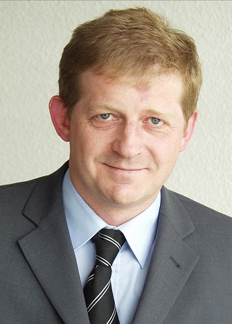
Speaker: Wolfgang Kunz (Technische Universitat Kaiserslautern)
Abstract:
This talk discusses the possible role of formal verification techniques in system-level design flows. In order to meet the challenges of the IoT era it is argued that the role of formal verification techniques should not be limited to "bug hunting" alone. Instead, formal technology should assume an entirely new role during the design process. It should be applied in such a way that a formal relationship is provided between an abstract system model and its concrete implementation at the Register Transfer Level (RTL). This will allow for new and highly effective approaches to achieving IoT-related design goals such as low power consumption and functional safety. The talk will present several industrial case studies demonstrating the potential of the proposed design methodology.
Biography:
Wolfgang Kunz received the Dipl.-Ing. degree in Electrical Engineering from the University of Karlsruhe, Germany, in 1989 and the Dr.-Ing. degree in Electrical Engineering from the University of Hannover, Germany, in 1992. From 1993 to 1998, he was with Max Planck Society, Fault-Tolerant Computing Group at the University of Potsdam, Germany. From 1998 to 2001 he was a professor of Computer Science at the University of Frankfurt/Main. Since 2001 he is a professor at the Department of Electrical & Computer Engineering at Technische Universitat Kaiserslautern.
Wolfgang Kunz conducts research in the area of System-on-Chip design and verification collaborating with several industrial partners including AbsInt, Alcatel-Lucent, Atrenta, Audi, Bosch, Infineon and OneSpin Solutions. For his research activities Wolfgang Kunz has received several awards including the Berlin Brandenburg Academy of Science Award and the Award of the German IT Society. Wolfgang Kunz is a Fellow of the IEEE.

Session 4 - Presentation 2
Title: Software in a Hardware View: New Models for Firmware Development and Safety Analysis in IoT Systems
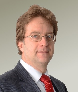
Speaker: Dominik Stoffel (Technische Universitat Kaiserslautern)
Abstract:
The Internet of Things builds upon large populations of embedded devices, many of which perform very specific, limited functions within a given application domain. There is a strong and increasing demand for small and efficient hardware/software computing platforms, at different tradeoff points for performance power consumption, and with strong requirements for safety and reliability. In highly competitive markets, ideally, the employed hardware/software platform should be nearly cost-optimal for the target application, and design productivity is a key factor for success. This poses great challenges for design and verification that can only be met with higher degrees of automation.
In this talk, we present a new computational model for hardware-dependent software that allows representing the execution behavior of a processor running low-level software such as the firmware in IoT devices. The model efficiently captures not only the effects of program execution but also the behavior at the hardware/software interface, as, for example, the interaction between the firmware and peripheral devices. We show and discuss applications of this model in firmware development and verification as well as in safety analysis.
Biography:
Dominik Stoffel obtained a Dipl.-Ing. degree from the University of Karlsruhe in 1992 and a Ph.D. from the University of Frankfurt in 1999.
From 1993 to 1994 he worked as an R&D engineer at Mercedes-Benz in the development of testing methodology for automotive electronics. From 1994 to 1998 he was with the Max-Planck Fault-Tolerant Computing Group in Potsdam. From 1998 to 2001 he was with the Electronic Design Automation group at the University of Frankfurt, Germany. Since 2001 he is working as a research scientist and lecturer in the Electronic Design Automation group at the University of Kaiserslautern. Dominik Stoffel conducts research in the area of design and verification of systems-on-chip. He has a special interest in methodologies and techniques for formal verification of hardware and low-level software. Dominik Stoffel has received the Award of the German IT Society.


VLSI Design and Education Center (VDEC), The University of Tokyo