The 8th VDEC D2T Symposium

October 24th (Thu.), 2013. 10:00-18:20
Takeda-Hall, 5th floor of Takeda Building, The University of Tokyo


Abstracts

Technologies and Platforms for Cyberphysical Systems
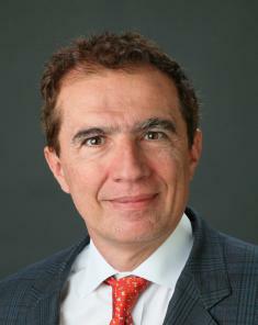
Prof. Giovanni De Micheli (Ecole Polytechnique Federale de Lausanne)
Much of our economy and way of living will be affected by nanotechnologies in the decade to come and beyond. Mastering materials at the molecular level and their interaction with living matter opens up unforeseeable horizons. This talk deals with how we will conceive, design and use cyberphysical systems exploiting devices at the edge of the scaling limits. Whereas switching circuits and microelectronics have been the enablers of computer and communication systems, new nano-devices have the potentials to realize innovative computational fabrics whose applications require broader hardware abstractions. Indeed, the first part on my talk will deal with a new type of electronic devices that act as atomic comparators, rather then switches. On this basis, a new flavor of circuit and logic synthesis is possible and effective.
In the second part of my talk I will address scaling of computing systems, and the current trend to manycore systems. Design complexity and usability will depend much on the interconnection schemes among computational elements. The technological feasibility envelope and the related multivariate design optimization problems find solutions in the network-on-chip choice as a general paradigm for circuit core interconnection.
Last I will describe cyberphysical system applications within the frame of the Swiss nano-tera.ch program. I will address the opportunities and limitations of current computing and communication systems toward addressing problems related to health management and environmental protection.

Test and Design-for-Testability Solutions for 3D Integrated Circuits
Prof. Krishnendu Chakrabarty (University of Tokyo / Duke University)
Despite the numerous benefits offered by 3D integration, testing remains a major obstacle that hinders its widespread adoption. Test techniques and design-for-testability (DfT) solutions for 3D ICs have remained largely unexplored in the research community, even though experts in industry have identified a number of hard problems related to the lack of probe access for wafers, test access to modules in stacked wafers/dies, thermal concerns, and new defects arising from unique processing steps. In this talk, the speaker will present a number of testing and DfT challenges, and describe some of the solutions being advocated for these challenges. The presentation will focus on the following hot topics:
- TSV defects and on-die defects induced by TSV processing, and test generation for TSV-induced stress;
- Pre-bond testing of TSVs and die logic, recent advances in probing, and non-invasive test using DfT;
- Post-bond testing and DfT innovations related to the optimization of die wrappers, test scheduling, and access to dies and inter-die interconnects;
- Fault diagnosis and TSV repair.
- Cost modeling and test-flow selection.

Activities of VDEC Advantest D2T Research Division (25 min.)
Prof. Satoshi Komatsu (University of Tokyo)
As the complexity of hardware functionality continues to increase, a test of VLSI chips becomes much more important. In such a situation, not only design of VLSI circuits but also testing of VLSI chips has become essential for the universities in terms of both research and education. To meet this trend, gAdvantest D2T research divisionh was established in VLSI Design and Education Center (VDEC) with the financial support of Advantest Corporation in 2007. In this talk, the goal of the D2T project and activities of the research division are briefly summarized.

Universal Methodology for Yield Enhancement of ULSIC's Employing Product Test, IC Layout and Comprehensive Suite of Characterization Vehicles
Prof. Andrzej Strojwas (Carnegie Mellon University / PDF Solutions Inc.)
Achieving the required time to market with economically acceptable yield levels and maintaining them in volume production has become a very challenging task in the most advanced technology nodes. In the older technology generations, manufacturing yield loss was dominated by random defects. By the time volume manufacturing started, systematic yield loss was typically insignificant. This situation started to change rapidly at the recent nodes in which the product layout systematic effects became more critical. More recently, due to challenging product performance requirements and increased process variability, parametric yield losses have become significant as well. We will present benchmarking of yield loss components for different product classes.
Then we will propose a comprehensive methodology for diagnosing yield loss mechanisms across technology lifecycle starting from technology development, process integration to new product introduction and volume manufacturing. This methodology employs a comprehensive suite of characterization vehicles that extract random and systematics defectivity levels and fail rates, as well as all the relevant process-layout interactions. The next crucial step in this methodology is the extraction of key layout attributes from the actual product layout or large IP cores if the product layout is not available yet. Then a comprehensive yield model can be developed with very high resolution to cover all important yield loss components. Analysis of product test results combined with an extensive set of scribe characterization vehicles allows then for a precise identification of a yield loss Pareto and then application of the necessary fixes. This methodology has been applied successfully industry-wide and we will illustrate its capabilities by real life examples from the most recent technology nodes down to 14nm FinFET processes and products.

Signal and Noise: A Radical Perspective on Mixed-Signal Test Research and Education
Prof. Mani Soma (University of Washington)
This presentation will emphasize the issues of mixed-signal design-for-test implementations on real mixed-signal circuits, as proposed by test researchers vs. as actually implemented by designers. Case studies will be presented to demonstrate the irony that mixed-signal design-for-measurement is a real success, not based on test research but based on designers' incorporation of calibration methods to ensure that their circuits work within specifications, in the presence of process variations and noise and other undesirable effects. We will elucidate the key factors for this success and the differences between design and test. In the meantime, mixed-signal test research has not kept pace with new design architectures, e.g. biomimetic designs, self-calibrated / self-healing mixed-signal designs, etc. A review of current mixed-signal test education shows minimal coverage in textbooks and courses and lack of emphasis on fundamental understanding of measurements. The presentation will conclude with some radical suggestions for future mixed-signal test research and education.

A Stochastic Sampling Time-to-Digital Converter
Dr. Takahiro J. Yamaguchi (Advantest Laboratories)
We introduce a stochastic time-to-digital converter (TDC) that has 180-770fs tunable resolution, less than 0.6LSB INL, and selectable dynamic range offset. Previous arbiter-based TDCs have fine resolution but small dynamic range which is difficult to calibrate. Our approach uses comparators as decision elements to precisely control dynamic range offset.

Synthesis from Oracles
Porf. Subash Shankar (University of Tokyo / City University of New York)
An exciting new design technique is the automatic synthesis of hardware from selected input/output pairs supplied by an oracle. This talk will discuss the approach, its successes and shortcomings, and a few ramifications on other aspects of design processes.

Layout Design for Practical Application of Electron-Beam Lithography with Character Projection Technique
Dr. Rimon Ikeno (University of Tokyo)
Electron Beam Direct Writing (EBDW) is expected as a low-cost solution of high-resolution lithography for its maskless feature. The biggest challenge in the practical EBDW application is to improve its low exposure throughput, and Character Projection (CP) technique is considered to be a promising approach for it due to its multi-figure exposure capability using character stencils.
In general, CP throughput is defined by the average figure number in the characters, but the character variation would explode easily if many, arbitrary layout figures are allowed in the characters. Then, we pursued design strategies realizing limited layout patterns, practical character variations, and practical CP throughput, including a new routing architecture, layout design methodologies, character-set plans, and stencil design methodologies. In this presentation, we discuss the details of our strategies and share the experimental results that support their feasibility in the practical CP application in the 14nm technology era.

Introduction of Multi-Purpose EB Lithography system F7000S
Mr. Masahiro Takizawa (Advantest)
We introduce the features of F7000S.
F7000S is EB lithography system which has Character Projection (CP) technology.
CP technology has some advantages compared with Variable Shaped Beam (VSB) system; (1) Shot count reduction by writing complex pattern in one CP shot, (2) high resolution by all pattern edges of CP shot coming from the edges of CP openings.
In addition, F7000S can handle the substrates of diverse size and shape (square, disk and chip of wafer) by Adjuster technology.

Panel Discussion "Challenges and Solutions for Future LSI Systems and Testing"
Moderator: Prof. Krishnendu Chakrabarty (University of Tokyo / Duke University)
Panelists:
Prof. Andrzej Strojwas (Carnegie Mellon University / PDF Solutions Inc.)
Prof. Giovanni De Micheli (Ecole Polytechnique Federale de Lausanne)
Prof. Mani Soma (University of Washington)
Dr. Takahiro J. Yamaguchi (Advantest Laboratories)
Panel Objectives and Description:

VLSI Design and Education Center (VDEC), The University of Tokyo