Last Updated:
Mon Jul 2 22:38:42 BST 2007
Japanese version is available.
Electron Beam Writer Mask System F5112+VD01
In the year 2004, VLSI Design and Education Center (VDEC) has got
an important donation from ADVANTEST corporation. The donation
included the state-of-the-art 8-inch electron beam (EB) direct
writer F5112. The EB machine is installed in the Federal Class
1
supercleanroom in Takeda building. The EB machine is opened
to academics since April 2005. Although ADVANTEST corporation now
proposes 300mm EB writing machine F3000 as their latest series,
the VDEC F5112 keeps offering quite comparable perfomance in terms
of EB pattern resolution.
After two academic years' common usage, total 71 students and
faculty staffs of more than 30 laboratoires, mainly from the
University of Tokyo, are licenced. Nearly 1000 exposures are
performed per year. As a consequence, competitiveness in MEMS
field of those groups are increasing. For example, F5112 user
laboratories share more than 13% of world's
papers*1 in MEMS conference
, which is the most important worldwide conference and the
acceptance ratio is quite low (5% for oral, 25% for poster
presentations).
The VDEC's EB support team is proud to underline that the
competitiveness is not only because of F5112's fine resolution and
rapid writing*2 characteristics,
but also because of the University of Tokyo Extention of the
apparatus; the UT version of F5112 (F5112+VD01) can write on
arbitral shapes and sizes of samples and photomasks (see below
for details).
From the year 2007, "Nanotech Network" funding program is launched
by Japanese Minstry of Education (METI). Our EB apparatus
participates as the U.Tokyo's network site together with Faculty
of Engineering's Electron Beam Microscopes cluster, including the
world's highest resolution Transmission Electron-Beam Microscope
(TEM). This program will help us to open the apparatus to even
more laboratories, especially extern to the U.Tokyo.
(*1) Example of MEMS2006 for Oral, 2007 for bothe Oral and Poster
MEMS2006 Oral:Total 41 papers/including U.Tokyo 8 papers/incl. F5112 group 5 papers.
MEMS2006 Poster:Total 186 papers/including U.Tokyo 13 papers/incl. F5112 group 9 papers.
MEMS2007 Oral:Total 43 papers/including U.Tokyo 6 papers/incl. F5112 group 6 papers.
MEMS2007 Poster:Total 142 papers/including U.Tokyo 20 papers/incl. F5112 group 19 papers.
(*2) Writing speed of F5112 is 10 to 100 times as fast as "ordinal
Electron Beam" writer. Nominal exposure time over 4 inch entire
wafer is within 30 minutes.
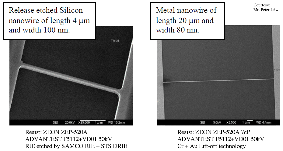
Exposure Example
The apparatus
-
- 1-1 Spin Coater SC-400
- Specification:
| Specification | Value |
|---|
| Rotation | 60 to 6000rpm |
|---|
| Steps | 2 steps |
|---|
- Placed on the chemical evacuation table.
- 1-2 Oven DNF-44
- Temperature 30 to 260 degree Celsius.
- Can accomodate up to 8 inch arbitrary shape can be put.
- Gas exhaust is possible.
-
- Specification
| Specification | Value |
|---|
| Guaranteed pattern resolution | 100nm |
|---|
| Pattern size tolerance | 15nm(3 sigma) |
|---|
| Field conjugation tolerance | Less than 40nm for
|average|+3 sigma |
|---|
| EB shape | Variable Square Beam and Character Block Exposure
|
|---|
- Functions
| Specification | Value |
|---|
| Acceleration | 50kV |
|---|
| Exposure Type | On-the-fly (OTF) exposure, Step &
repeat (SR) exposure. Stage is deceleratable for large shot numbers.
|
|---|
| Wafer size | up to 8 inch round |
|---|
| Loader | Single |
|---|
- Sample size (Unique feature of VD01)
- 4 inch (4009) quartz mask
- 5 inch (5009) quartz mask
- 2 inch 270um-thick round wafer
- 3 inch 380um-thick round wafer
- 4 inch 525um-thick round wafer
- 1.0x1.0 to 3.0x3.0cm arbitral shape wafers (thickness: 325um,
425um, 525um, or 725um)
- 8 inch 725um-thick round wafer (*)
Other size and thickness can be accomodated by preparing dedicated adjuster.
(* Alignment mark is obligatory on the wafer.)
-
- 3-1 Wet Mask Developer APT3150
- Can accomodate 3,4,5,6,7inch mask blank and 3,4,5,6,7inch round wafers.
- Includes chemical exhaust system.
- Automatic development, rinsing, and spin-dry.
- 3-2 Wet Mask Etcher APT1140
- Can accomodate 3,4,5,6,7inch mask blank and 3,4,5,6,7inch round wafers.
- Automatic development, rinsing, and spin-dry.
-
- 4-1 Cleaner
- Can accomodate 3,4,5,6,7inch mask blank and 3,4,5,6,7inch round wafers.
- Automatic H2SO4 cleaning, scrub cleaning, rinsing, and spin dry.
- 4-2 Plasma Asher PAC-III
- Can accomodate 3,4,5,6,7inch mask blank and 3,4,5,6,7inch round wafers.
- Two mass flow control system.
- Short turn around time.
-
- 5-1 LASER Microscope
- Features below:
| Specification | Value |
|---|
| Resolution | 0.25um |
|---|
| Light Source | He-Ne LASER |
|---|
| Scan Frequency | Horizontal 15.73kHz Vertical 60Hz |
|---|
| Least Significant Bit of scale | 0.001um |
|---|
| Scale Error | plus minus 0.03um |
|---|
| gamma correction | possible |
|---|
- LASER scanning microscope, motor driven stage, antivibration stage, and monitor.
- 3 dimensional image processing software bundled.
- Stage is addressable by plus minus 2 micron resolution.
 Back to top page
VDEC Home Page / Univ. of Tokyo. /
equipment at vdec.u-tokyo.ac.jp