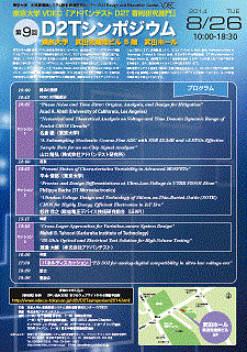
The 9th D2T Symposium, VDEC, The University of Tokyo

August 26th (Tue.), 2014. 10:00-18:30
Takeda-Hall, 5th floor of Takeda Building, The University of Tokyo

(日本語版, Japanese version)


News:

- Symposium is over. Thank you very much. (2014/8/26)
- Symposium poster is linked. (2014/7/22)
- Presentation abstracts are linked. (2014/7/10)
- Registration is started. (2014/6/16)
- The symposium program is disclosed. (2014/6/13)
- The symposium homepage is opened. (2014/5/30)


Symposium Overview

Organizer VLSI Design and Education Center (VDEC), The University of Tokyo
Sponsor ADVANTEST Corporation
Supporters The Institute of Electronics, Information and Communication Engineers (IEICE)
Information Processing Society of japan (IPSJ)
IEEE SSCS Japan Chapter
Japan Electronics and Information Technology Industries Association (JEITA)
SEMI Japan
Semiconducto Equipment Association in Japan (SEAJ)
The Institute of NANO Testing (INANOT)
Power Device Enabling Association (PDEA)
Admission fee Not required

Symposium Program (日本語版, Japanese version)

10:00 Opening remarks
10:15 Activities of VDEC Advantest D2T Reseach Division
10:25 Session 1
Phase Noise and Jitter in Circuits: Origins, and How They Affect Signals [Invited]
Asad A. Abidi (University of California, Los Angeles)
Numerical and Theoretical Analysis on Voltage and Time Domain Dynamic Range of Scaled CMOS Circuits
Toru Nakura (The University of Tokyo)
A Subsampling Stochastic Coarse-Fine ADC with SNR 55.3dB and >5.8TS/s Effective Sample Rate for an on-Chip Signal Analyzer
Takahiro J. Yamaguchi (Advantest Laboratories)
12:00 Lunch
13:15 Session 2
Present Status of Characteristics Variability in Advanced MOSFETs [Invited]
Prof. Toshiro Hiramoto (The University of Tokyo)
Process and Design Differentiations at Ultra-Low-Voltage in UTBB FDSOI 28nm [Invited]
Philippe Roche (ST Microelectronics)
Ultralow-Voltage Design and Technology of Silicon-on-Thin-Buried-Oxide (SOTB) CMOS for Highly Energy Efficient Electronics in IoT Era [Invited]
Nobuyuki Sugii (Low-power Electronics Association & Project)
15:15 Coffee Break
15:45 Session 3
Cross-Layer Approaches for Variation-aware System Design [Invited]
Mehdi B. Tahoori (Karlsruhe Institute of Technology)
30-Gb/s Optical and Electrical Test Solution for High-Volume Testing
Daisuke Watanabe (Advantest Corporation)
16:50 Break
17:00 Panel Discussion
Theme: FD SOI for analog-digital compatibility in ultra-low voltage era
18:20 Closing remarks
18:30 Banquet

Registration (Free)

Please register HERE.(Japanse page)
This symposium is over. Thank you.


Access to the Symposium

Please look at the MAP.


Contact

ADVANTEST D2T Research Divison,
VLSI Design and Education Center (VDEC), The University of Tokyo
Room 404, Takada Building, Yayoi 2-11-16, Bunkyo-ku, Tokyo, 113-8656, Japan
Tel: +81-3-5841-0233 FAX: +81-3-5841-1093
E-mail: ikeno@vdec.u-tokyo.ac.jp


VLSI Design and Education Center (VDEC), The University of Tokyo